In the intricate world of electronics manufacturing, soldering technologies serve as the foundation for reliable circuit board assembly. Among the most prominent methods are reflow soldering and wave soldering, each with distinct mechanisms, applications, and performance characteristics. For manufacturers and engineers, understanding the differences between these two processes is essential for optimizing production quality, efficiency, and cost-effectiveness. This guide breaks down their core distinctions, helping you determine which technology best suits your specific manufacturing needs.
Table of Contents
Toggle1.Fundamental Working Principles
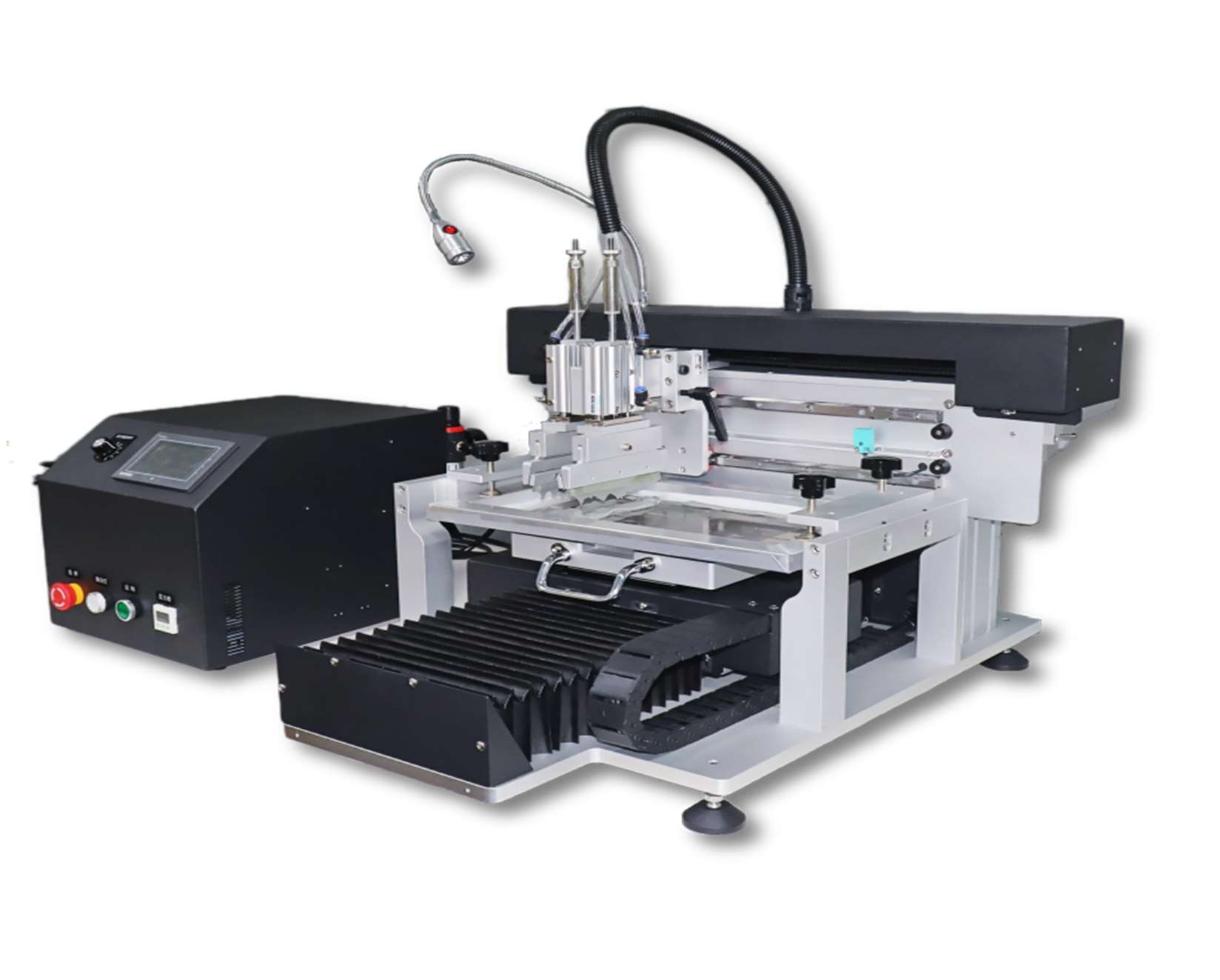
a.How Reflow Soldering Works:
- Preheat stage: Gradually raises the temperature to evaporate solvents in the solder paste and activate the flux, which removes oxide layers from metal surfaces.
- Reflow stage: Reaches the solder alloy’s melting point (typically 217–225°C for lead-free formulations), causing the paste to liquefy and form strong metallurgical bonds between components and PCB pads.
- Cooling stage: Rapidly cools the board to solidify the solder, creating durable, electrically conductive joints.
b.How Wave Soldering Works:
Wave soldering, by contrast, is a bulk soldering process primarily intended for through-hole technology (THT) components. The process starts with flux application to the PCB’s bottom side, either through spray, foam, or dip methods, to prevent oxidation during soldering.
After flux application, the PCB enters a preheating zone to activate the flux and minimize thermal shock when contacting molten solder. The key stage involves passing the PCB over a continuous wave of molten solder (maintained at 250–270°C for lead-free alloys) generated by a pump system.
As the PCB travels over the wave, the molten solder rises through the through-holes, forming fillets around component leads and creating reliable solder joints. Excess solder drains off as the board exits the wave, and the solder solidifies as the PCB cools, completing the process.
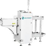
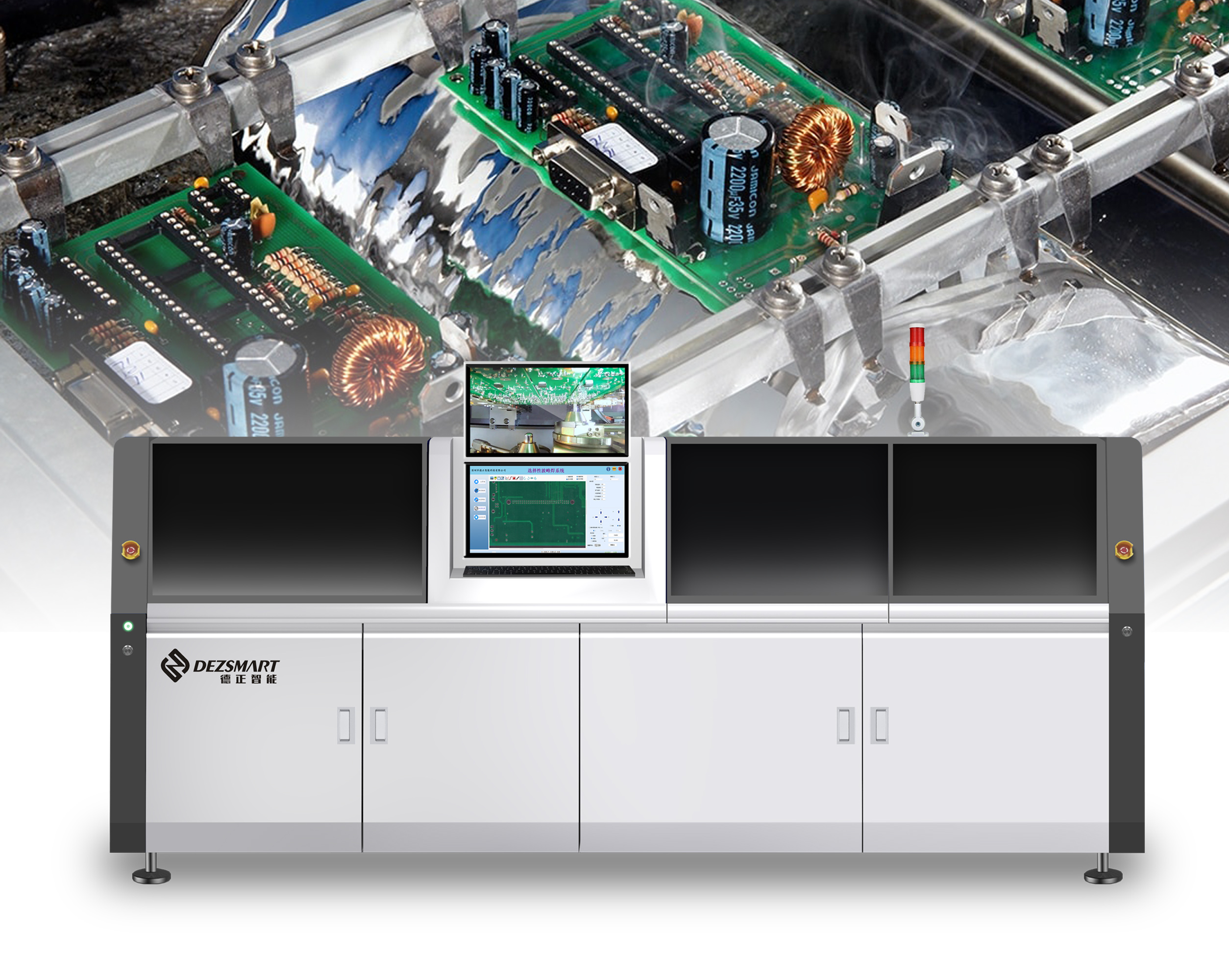
Modern variations like selective wave soldering target specific areas of the PCB, allowing for more precise application and compatibility with mixed-technology boards containing both through-hole and surface-mount components.
2.Component Compatibility
- Small passive components: resistors, capacitors, inductors
- Integrated circuits (ICs) in various packages: QFP (Quad Flat Pack), BGA (Ball Grid Array), CSP (Chip Scale Package)
- SMD connectors and switches with surface-mount terminals
- LED packages and small sensors
- Power connectors and terminal blocks
- Electrolytic capacitors with long leads
- DIP (Dual In-line Package) ICs
- Relays, transformers, and other bulky components
- Fuses and connectors requiring high mechanical strength
3.Process Control and Precision
a.Reflow Soldering Control Factors
Reflow soldering requires meticulous control over multiple variables to ensure quality results:
- Solder paste deposition: The accuracy of stencil printing directly impacts joint quality, with factors like stencil thickness, aperture size, and printing pressure requiring precise calibration.
- Temperature profiling: Oven zones must be carefully adjusted to match the solder paste’s requirements, with heating rates typically limited to 2–3°C per second to prevent component damage.
- Component placement: Misalignment of just 0.1mm can cause soldering defects in fine-pitch components, necessitating high-precision pick-and-place equipment.
Advanced reflow ovens feature closed-loop temperature control and nitrogen atmospheres to reduce oxidation, enabling consistent results even for high-density PCBs with thousands of solder joints.
b.Wave Soldering Control Factors
Wave soldering quality depends on different critical parameters:
- Flux coverage: Uniform application is essential to prevent oxidation; insufficient flux leads to dry joints, while excess flux can cause contamination.
- Wave parameters: Wave height, velocity, and temperature must be optimized for the PCB design—too high a wave causes bridging between adjacent leads, while insufficient contact time results in cold joints.
- Conveyor speed: Typically set between 0.5–1.5 meters per minute, the speed determines solder contact time (usually 2–4 seconds) and must be matched to board complexity.
Selective wave soldering systems enhance precision by using programmable nozzles to target specific areas, allowing for controlled solder application even on PCBs with sensitive components.
4.Defect Profiles and Quality Control
a.Common Reflow Soldering Defects
Reflow processes are susceptible to specific defects related to thermal management and material handling:
- Tombstoning: Small components (especially resistors and capacitors) stand upright due to uneven solder paste application or unequal heating.
- Solder balls: Tiny spheres of solder on the PCB surface, caused by excessive paste, improper stencil alignment, or insufficient preheating.
- Insufficient wetting: Poor adhesion between solder and pads, often resulting from oxide layers not removed by flux.
- Bridging: Solder connecting adjacent pads, particularly problematic in fine-pitch ICs.
These defects are managed through rigorous process control, including solder paste inspection systems and real-time temperature monitoring.
b.Common Wave Soldering Defects
Wave soldering defects typically relate to solder flow and board handling:
- Bridging: Excess solder connecting adjacent through-holes, requiring manual repair.
- Cold joints: Dull, granular joints with poor electrical conductivity, caused by insufficient heat or flux activation.
- Solder skips: Missing joints due to blocked holes, inadequate flux, or poor wave contact.
- Dross inclusions: Oxidized solder particles trapped in joints, weakening them and causing reliability issues.
Modern wave soldering machines mitigate these issues with features like nitrogen inerting, improved fluxing systems, and wave profiling technologies.
5.Application Scenarios
a.Best Uses for Reflow Soldering
Reflow soldering is the technology of choice in:
- Consumer electronics: smartphones, tablets, wearables, and laptops featuring high-density SMD components.
- Telecommunications: 5G equipment, routers, and network devices with complex ICs.
- Automotive electronics: Advanced driver-assistance systems (ADAS) and infotainment systems with miniaturized components.
- Medical devices: Portable monitors and diagnostic equipment requiring reliable, compact assemblies.
b.Best Uses for Wave Soldering
Wave soldering excels in applications including:
- Industrial controls: Motor drives, power supplies, and control panels with rugged through-hole components.
- Automotive electronics: Power distribution modules and sensor connectors requiring robust joints.
- Aerospace and defense: High-reliability systems with through-hole components for enhanced vibration resistance.
- Appliances: Control boards for white goods with a mix of through-hole connectors and discrete components.
6.Conclusion: Choosing the Right Technology
- Choose reflow soldering for SMD-dominated, high-density PCBs requiring fine-pitch precision.
- Choose wave soldering for through-hole components and mixed-technology boards where robust mechanical joints are critical.